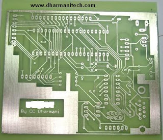
Home-made Double Layer ATmega32 PCB for RS232/RS422 Communication testing


Hi guys,
after making my single layer starter's kit M32_Card, I was looking for making a double layer M32 PCB at home. So, here is my attempt to make it. Well, it didn't turn out to be as difficult as I had thought it to be earlier. I had to dump one PCB before making this one as the top-layer routine was not solder-friendly!!
I've made this one mainly for an application where RS232 & RS422 testing was required. It uses MAX232 & MAX488 ICs from for those serial communication. Selection between RS232 & RS422 is through jumpers. The board is using ATmega32 controller, just like my single layer pcb. It also has 4x4 matrix keyboard, an LCD interface, ADC connector, SPI connector (for In System Programming), a reset switch and an LED for beginner's programming. It operates with the standard 12v DC adapter.
I've made this one mainly for an application where RS232 & RS422 testing was required. It uses MAX232 & MAX488 ICs from for those serial communication. Selection between RS232 & RS422 is through jumpers. The board is using ATmega32 controller, just like my single layer pcb. It also has 4x4 matrix keyboard, an LCD interface, ADC connector, SPI connector (for In System Programming), a reset switch and an LED for beginner's programming. It operates with the standard 12v DC adapter.
Here is the schematic (click on the image to enlarge):

There is a small mistake here in the schematic, the RX/TX pin connections in the RS232 connector are swapped, which I found while testing the PCB. So, I had to correct it by cutting those two tracks and placing jumpers. After the correction, the communication with PC was established. The schematic is similar to the M32_Card, accept that I've removed the RTC DS1307 and placed the MAX488. Also, the individual push buttons are replaced with the 16 key matrix key-board.
Click here to get more info and for downloading code to interface the 4x4 matrix keyboard shown here
The PCB etching is done with Ferric Chloride. In making the double layer PCB, as I don't have any PTH (printed through holes) facility, I've put small pieces of single core wire into the holes and soldered both sides. Check out the top and bottom layers here


If you have an application where the circuit can not be contained in a single layer, a home-made double layer PCB is worth a try!!
Thanks!


No comments:
Post a Comment